This isn't necessarily the final answer. You haven't supplied enough information with your question to determine whether your oscillation is caused by one or both of two possible causes.
I had made changes to your originally supplied code:
entity dfff is
    port (
        d,clk1:    in    bit;
        qd,qnd:    inout bit
    );
end entity;

architecture foo of dfff is

begin
    process (clk1)
    begin
        if clk1'event and clk1 = '1' then
            qd  <= d;
            qnd <= not d;
        end if;
    end process;
end architecture;


-- library ieee;
-- use ieee.std_logic_1164.all;
entity ccou is
    port (
        clk2:           in  bit;
        qa,qb,qc:       out bit; -- inout
        cqd:            out bit;     -- inout
        qna,qnb,qnc:    out bit; --inout
        cqnd:           out bit  -- inout bit := '1' -- ); -- inout
    );
end entity;

architecture a_ccou of ccou is
    component dfff
        port (
            d,clk1: in    bit;
            qd,qnd: inout bit
        );
    end component;

--    signal ta: bit;

    signal iqa, iqb, iqc, icqd:  bit;
    signal iqna, iqnb, iqnc, icqnd: bit;
begin
    qa <= iqa;
    qb <= iqb;
    qc <= iqc;
    cqd <= icqd;
    qna <= iqna;
    qnb <= iqnb;
    qnc <= iqnc;
    cqnd <= icqnd;

g1: dfff port map (icqnd, clk2,  iqa,  iqna);
g2: dfff port map (iqa,   clk2,  iqb,  iqnb);
g3: dfff port map (iqb,   clk2,  iqc,  iqnc);
g4: dfff port map (iqc,   clk2, icqd, icqnd);
end architecture;

entity ccou_tb is
end entity;

architecture foo of ccou_tb is
    signal clk2: bit;
    signal qa, qb, qc, cqd, qna, qnb, qnc, cqnd: bit;
begin
CLOCK:
    process
    begin
        wait for 10 ns;
        clk2 <= not clk2;
    end process;

DUT:
    entity work.ccou
        port map (
            clk2 => clk2,
            qa => qa,
            qb => qb,
            qc => qc,
            cqd => cqd,
            qna => qna,
            qnb => qnb,
            qnc =>  qnc,
            cqnd => cqnd
        );

end architecture;
The changes provided mode out on ccou, adding internal signals, a behavioral model of the dfff flip flop and, a testbench.
That produced:
 (clickable)
This is pretty much telling us you have a problem with your dfff flip flop entity/architecture. Note the behavioral dfff model uses an edge clock.
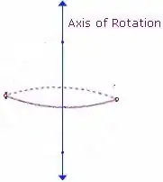
Note your added chalkboard drawing image matches
from the Microarchitecture of Pipelined and Superscalar Computers, 1999 by Amos R. Omandi. And represents a D Latch, not an edge sensitive flip flop.
S R latch feedback oscillation
If your dfff is indeed based on your chalkboard representation one source of oscillation can be remedied by unbalancing the Q BAR to S and Q to R delays on the R S latch or by using a consensus term in an Earle latch.
Essentially when clk1 is false in your dfff implementation SR latch might oscillate because the feed back inputs have events at the same time.
The Earle latch:

uses a consensus term (the middle AND gate) to dampen S R latch oscillation, keeping the output high when the input is high and represents a real world solution that happens to lend itself to simulation.
In device physics we also have the ability to unbalance delays be trimming trace capacitance or transistor size.
Here the S R latch feedback oscillation is a modelling shortcoming that is useful for teaching real design issues.
Enabled Ring delay plus inversion
Unfortunately the ring counter implemented with 'transparent' latches is also susceptible to an oscillation when clk1 (the enable) is true and the ring feedback (g4 qnd output to g1 d input) provides inversion.
We used to call this a striking oscillator, a gated relaxation oscillator.
Fixing the ring feedback oscillation requires using an edge sensitive flip flop or non-overlapping clocks between successive flip flops, preventing a less than 4 clock delay around ring.
See the Wikipedia Master–slave edge-triggered D flip-flop.
A master slave flip flop is implemented with two successive D latches one operating off one phase of the clock (as an enable) and the other off the opposite phase.
These can have requirements for unbalanced feedback delay in the S R latches. The gate level representation shown provides that, plus there are other representations that minimize gate delays.
About now you might get the idea this is a hardware design issue.