2

Context: I am following an embedded systems course https://www.edx.org/course/embedded-systems-shape-the-world-microcontroller-i

In the lecture on bit specific addressing they present the following example on a "peanut butter and jelly port".

Given you a port PB which has a base address of 0x40005000 and you wanted to access both port 4 and port 6 from PB which would be PB6 and PB4 respectively. One could add the offset of port 4(0x40) and port 6(0x100) to the base address(0x40005000) and define that as their new address 0x40005140.

Here is where I am confused. If I wanted to define the address for PB6 it would be base(0x40005000) + offset(0x100) = 0x40005100 and the address for PB4 would be base(0x40005000) + offset(0x40) = 0x40005040. So how is it that to access both of them I could use base(0x40005000) + offset(0x40) + offset(0x100) = 0x40005140? Is this is not an entirely different location in memory for them individually?

Also why is bit 0 represented as 0x004. In binary that would be 0000 0100. I suppose it would represent bit 0 if you disregard the first two binary bits but why are we disregarding them?
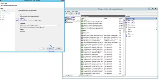
Lecture notes on bit specific addressing: enter image description here

Clifford
  • 88,407
  • 13
  • 85
  • 165
  • 1
    Your questions and interpretation seem reasonable. The quoted text looks like complete rubbish. There are basic errors in English and they are confusing the terms port and pin (or port and pad). Did you copy+paste it exactly or have you re-typed it and maybe made a mistake? – Tom V Dec 16 '22 at 18:40
  • Does the course mention anything about memory-mapped I/O? – Jim Rhodes Dec 16 '22 at 18:47
  • Let me clarify that it would be Port PB and we would be accessing Pin 4 and Pin 6. My mistake and the quoted text is just to illustrate an example port PB. The course does mention memory-mapped I/O and the microcontroller we are using is the Tiva™ TM4C123GH6PM . – Eric Kemmer Dec 16 '22 at 19:52
  • You need to mention the TM4C123GH6PM in the question itself. The behaviour is peculiar to that device family. In that sense a poor example for a general course, that "trick" is not generally applicable. – Clifford Dec 17 '22 at 10:57

1 Answers1

5

Your interpretation of how memory-mapped registers are addressed is quite reasonable for any normal peripheral on an ARM based microcontroller.

However, if you read the GPIODATA register definition on page 662 of the TM4C123GH6PM datasheet then you will see that this "register" behaves very differently.

They map a huge block of the address space (1024 bytes) to a single 32-bit register. This means that bits[9:2] of the the address bus are not needed, and are in fact overloaded with data. They contain the mask of the bits to be updated. This is what the "offset" calculation you have copied is trying to describe.

Personally I think this hardware interface could be a very clever way to let you set only some of the outputs within a bank using a single atomic write, but it makes this a very bad choice of device to use for teaching, because this isn't the way things normally work.

R S
  • 162
  • 3
  • 11
Tom V
  • 4,827
  • 2
  • 5
  • 22
  • I see now that the address bits to be updated are bits[9:2], and you mention "they are not needed" in the sense they are not reserved by the register so we can in fact use them for our purposes if I understand you correctly. I am not clear on how "they contain the mask of the bits to be updated". Page 654 of the [TM4C123GH6PM](https://www.ti.com/lit/ds/symlink/tm4c123gh6pm.pdf) data sheet gives some examples of how one can read or write to this register but method is still confusing to me. – Eric Kemmer Dec 17 '22 at 16:53
  • 1
    Bits 9:2 of the address are not needed in order in the sense that they are not required to work out which register you want to access. – Tom V Dec 17 '22 at 19:37
  • 1
    To explain further: a 32 bit register is 4 bytes. They have allocated 1024 bytes worth of addresses. This is 256 times as many as is needed. By selecting one of those 256 options you are able to write 40 bits of data to the register. 32 bits on the data bus, and 8 bits on the address bus. this leaves only 22 bits at the top of the address bus to contain the actual register address, and two bits at the bottom to optionally select bytes within the register. – Tom V Dec 17 '22 at 19:38